At the world’s largest photonics technologies event in San Francisco, California, Jenoptik will be presenting its broad product portfolio of high-performance optical components and systems, which serve current trends in medical, laser, optoelectronics, semiconductor equipment, data transmission and imaging technology.
To discover how Jenoptik’s technologies enhance our lives with smarter photonic solutions, visit them January 27 – February 1 at the SPIE trade shows:
- SPIE BiOS: Jenoptik and SwissOptic booth #8636 from January 27 to 28
- SPIE AR|VR|MR: TRIOPTICS booth #6312 from January 29 to January 31
- SPIE Photonics West: Jenoptik and SwissOptic booth #1341 and TRIOPTICS, a member of the Jenoptik Group, booth #1441 from January 30 to February 1.
To schedule a meeting or for more information please visit our event website.
Images are available in the Jenoptik image database in the “Press Release” section.
Introducing the novel single-bar diode laser package LS
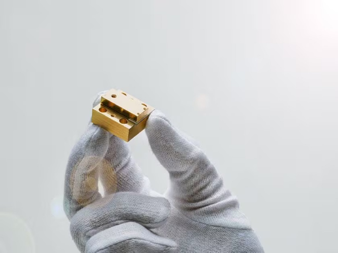
Jenoptik is introducing its novel open heat sink diode laser package “LS” for optical pumping of next-generation solid-state-lasers, which offers significantly increased optical output power levels compared to the industry-standard CS.
While only slightly deviating from the CS form factor, the LS features improved conductive cooling of the laser bar by virtue of a double-side cooled open heat sink design. As a result, the LS offers superior performance compared to the CS with cw-output power levels exceeding 150 W @ 9xx nm thus enabling advanced pump- or direct-diode-laser (DDL) applications.
Featuring an almost identical form factor as the CS-package, Jenoptik’s LS package offers upgrade capability of already existing (pump) assemblies based on the CS with the benefit of boosting optical (pump) power to unprecedented levels.
Join them for a live demonstration of our white light source technologies for medical technology and life science
To further support future image-guided surgical procedures as well as diagnostic imaging applications e.g. based on digital microscopy, Jenoptik has developed a solid-state-based color-gamut tunable (white) light source which allows for high-brightness illumination at virtually any chromaticity setting.
Color-gamut tuning via mixing of three or more independent color-channels allows for imaging under different (multi-)spectral illumination conditions and thus enables improved visual discrimination for the surgeon and/or future AI-based image-processing-algorithms. For minimally invasive endo-illumination e.g. in ophthalmic surgery, the high beam quality of the (white) light source supports gauge sizes beyond 27G.
Join them at our booth for a live demonstration of our white light source technologies, and for an exchange on your specific needs for smart illumination in your next-generation surgical or diagnostic imaging device – may it be in ophthalmology, urology, gynecology and/or endoscopy.
Furthermore, don’t miss our imaging solutions expert Hannes Weise’s presentation “High quality imaging in small spaces: endoscopes for OEM integration” on January 28th at 4:20 p.m. PST.
Opto-electronic solution for PIC testing on wafer level
With the opto-electronic UFO Probe® Card, Jenoptik offers wafer manufacturers and wafer test equipment suppliers a timesaving and yield-increasing solution for the synchronized testing of electronic and photonic components.
Jenoptik’s Probe Card enables the simultaneous testing of electrical and photonic functionalities at wafer level – especially at high throughput rates in high-volume production. The innovative optical test concept of the UFO Probe® eliminates the need for active alignment. Each UFO Probe® Card is customized to the individual requirements and the respective wafer layout and is available with both cantilever and vertical needle technology. It covers the wavelength range from 1260 to 1625 nanometers used in the telecommunications and data communications sector, including polarization maintaining for individual or all optical channels.
By incorporating the vertical needle technology, Jenoptik has responded to the increased market requirements, particularly regarding co-packaged optics and ensures the economical use of the UFO Probe® in high-volume test scenarios and ATE operability.
Supporting photonics entrepreneurs in the SPIE Startup Challenge
Jenoptik will also be one of the main sponsors of the SPIE Startup Challenge, a competition for photonics entrepreneurs to pitch their light-based technology business plans to industry experts. Hosted by SPIE, the international society for optics and photonics, the startup challenge’s final presentations will take place during the Photonics West show on January 30, 2024. Founding partner Jenoptik will once again support the event with expertise and cash prizes, which will be awarded to the top three finalists.
Image: Novel open heat sink diode laser package “LS” for optical pumping of next-generation solid-state-lasers.
About Jenoptik and its Advanced Photonic Solutions division
Optical technologies form the basis of our business. Jenoptik is a global photonics group and comprises the two divisions Advanced Photonic Solutions and Smart Mobility Solutions. Our key markets primarily include semiconductor & electronics, life science & medical technology as well as smart mobility. More than 4,400 people worldwide work for the Jenoptik Group, which is headquartered in Jena (Germany). JENOPTIK AG is listed on the German Stock Exchange in Frankfurt and traded on the MDax and TecDax. In fiscal year 2022, Jenoptik generated revenue of 980.7 million euros.
The Advanced Photonic Solutions division of Jenoptik is a global OEM and machine supplier of solutions powered by photonics. Our expertise excels across a broad portfolio of technologies in the fields of optics, laser technology, digital imaging, optoelectronics, sensors, and optical test & measurement equipment. Our systems, modules and components put our customers in the lead by helping them master their future challenges through the power of light.
