Investment in new production tool for the semiconductor equipment industry.
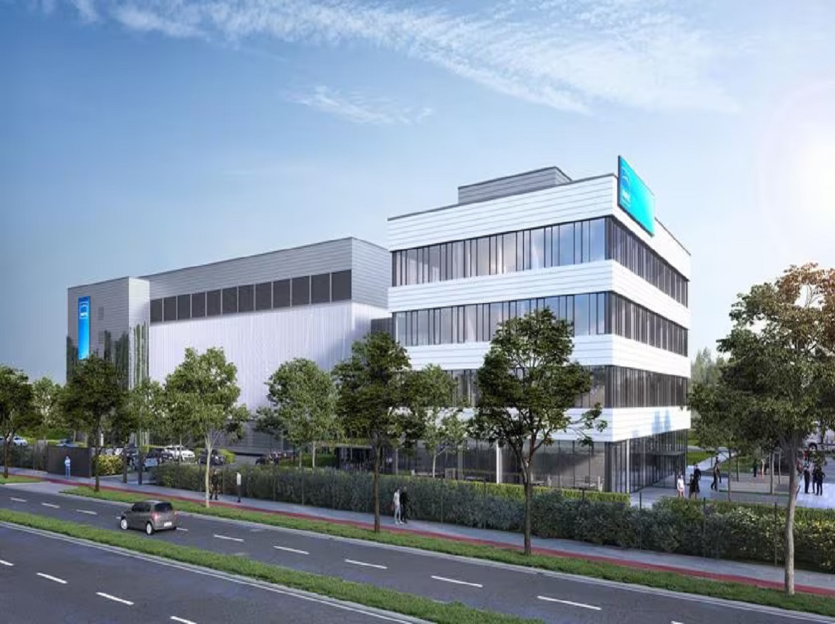
Jenoptik is investing a low double-digit million-euro amount in a state-of-the-art system for the high-tech fab currently under construction in Dresden. The new electron-beam lithography system (E-Beam) will be used to manufacture high-precision micro-optical components for customers in the semiconductor and optical communication sectors. The manufacturer is the Jena based e-beam technology specialist Vistec Electron Beam GmbH. The system will be delivered at the beginning of 2025.
Creating the smallest structures with maximum precision
This type of electron-beam lithography system can “write” structures with a precision in the 10-nanometer range (approximately 1/2,000th of a hair) on substrates up to 300 mm in diameter.
The Vistec SB3050-2 electron-beam lithography system is based on the so-called Variable Shaped Beam principle, with which even large areas can be structured highly accurately and effectively. The high degree of automation, combined with flexibility in terms of usable substrates, are further features of the Vistec SB3050-2 that enable it to be used in an industrial environment. The system is equipped with Cell Projection functionality, opening up further possibilities for applications in micro-optics.
Jenoptik has been active in Dresden since 2007. With the new high-tech fab at Airportpark Dresden, the company is consolidating its production, which is currently spread across several small external sites, while at the same time expanding its capacities. The clean room production in the new fab will cover 2,000 square meters with clean room areas of classes ISO 5 and 3 and meet the highest requirements for freedom from vibrations and temperature stability.
High environmental standards are taken into account for the entire fab: Jenoptik is striving to fulfill the currently most comprehensive and stringent building criteria in terms of sustainability with the “KfW 40 Standard” and the “LEED Gold Standard Certification”. At the same time, high-quality jobs will be created and the number of employees on site will increase to a total of more than 120. The Saxon state capital will thus become the main location for the micro-optics sector.
About Jenoptik
Optical technologies form the basis of our business. Jenoptik is a global photonics group and comprises the two divisions Advanced Photonic Solutions and Smart Mobility Solutions. Non-photonic activities, particularly for the automotive market, are operated as independent brands within the Non-Photonic Portfolio Companies. Our key markets primarily include semiconductor & electronics, life science & medical technology as well as smart mobility. More than 4,400 people worldwide work for the Jenoptik Group, which is headquartered in Jena (Germany). JENOPTIK AG is listed on the German Stock Exchange in Frankfurt and traded on the MDax and TecDax. In fiscal year 2022, Jenoptik generated revenue of 980.7 million euros.
About Vistec Electron Beam GmbH
As a long-standing equipment supplier, Vistec Electron Beam GmbH, Jena (Germany) is providing leading technology solutions for advanced electron-beam lithography. Based on the Variable Shaped Beam (VSB) principle, the electron-beam lithography systems are mainly utilized for industrial and advanced research applications, such as electron-beam direct write in semiconductor manufacturing, including compound semiconductor direct write, mask writing as well as photonics and several new emerging markets. Efficient data processing & innovative exposure strategies (e.g. Cell Projection) open up new applications, especially in the field of AR/VR. Vistec’s technology features automated handling, as well as high flexibility, writing accuracy and productivity and therefore is suitable for prototyping and low volume production. In addition to its production facility in Germany, Vistec maintains service & support centers in Asia Pacific, USA and Europe.
