
Semiconductor fabrication is a multi-step manufacturing process that combines mechanical, photolithographic, and chemical processing procedures. On a wafer formed of pure semiconducting material, electronic circuits are gradually built during this process. Although other compound semiconductors are preferred for specialized purposes, silicon is almost always employed.
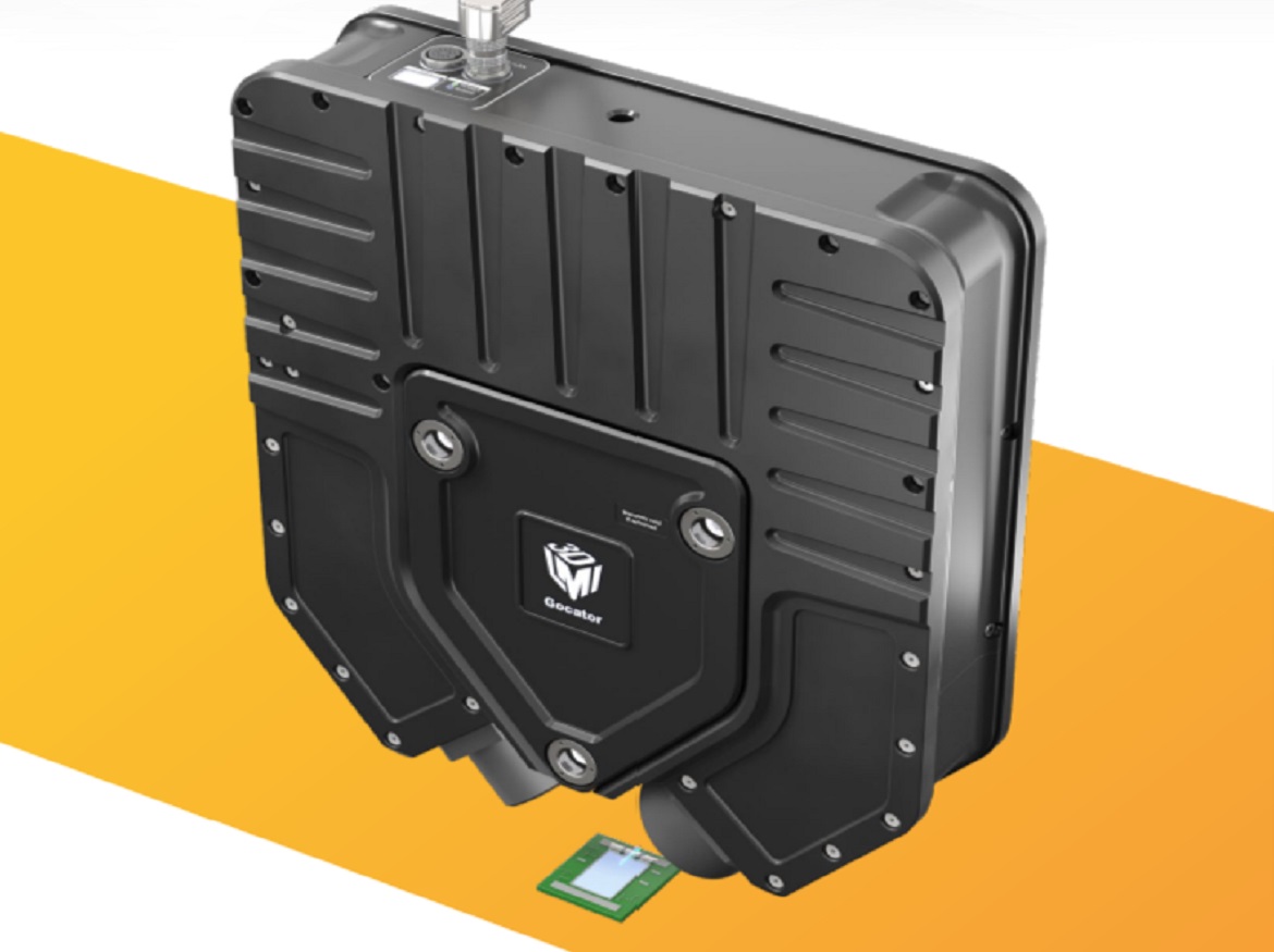
For maximum product quality and optimum production throughput, Gocator® 3D Line Confocal Sensors enable precise inline 3D scanning and inspection at various phases of this fabrication process.
THE SEMICONDUCTOR FABRICATION PROCESS
1. Wafer sorting
Wafers are divided into various varieties based on a set of criteria. The form, length, width, thickness, and surface flaws of silicon wafers must all be under strict quality control during this classification procedure.
Wafer size, thickness, and flatness are scanned and examined using Gocator® 3D Line Confocal Sensors, which also offer highly accurate defect identification.
1.1 Wafer polishing pad inspection
The chemical-mechanical polishing (CMP) process is balanced in a significant way by the wafer polishing pads. These pads eventually start to show wear, thus routine inspections are required as part of the production line’s machine monitoring protocol.
You can scan the wafer pad’s surface using Gocator® 3D Line Confocal Sensors to look for any potential variations in 3D height data that might point to wear-prone spots.
2. Wafer dimensional measurement and defect detection after scribing
An example of a die singulation technique is scribing, in which a process instrument (such as a laser or saw blade) partially cuts through a wafer or substrate before separating it into an individual die in a subsequent “breaking” step. To achieve precise wafer cutting during this manufacturing process, the die must undergo a complete surface examination.
Gocator® 3D Line Confocal Sensors are used to monitor the precision of the groove placement, groove depth, and kerf width of the wafer scribing after laser dicing and/or scribing is finished in order to avoid flaws such as die chipping. As a result, there are more usable dies per wafer, and the best processing quality and throughput are guaranteed.
3. Inspection of BGA and PGA position, height, and radius during assembly and test IC
BGA
A common integrated circuit (IC) chip, the BGA (Ball Grid Array) chip uses SMT (Surface Mount Technology) to provide high-density connectivity. BGA balls are dispersed across the bottom surface of the chip, allowing for an increase in ball count while maintaining a constant chip volume. Inspection of pin height, diameter, offset, and missing solder is necessary due to the growing use of BGA pins in semiconductor fabrication.
With a ball diameter of less than 50 m, Gocator® 3D Line Confocal Sensors can precisely measure the ball’s height, position, and other dimensions.
PGA
PGAs (Pin Grid Array) are made up of a number of square matrix pins that are positioned at specific intervals along the chip’s edge and are found both inside and outside the chip. The PGA can be encircled in circles with two to five pins, depending on the number of pins. PGAs are larger than BGAs, but they are also simpler to replace, and some operational faults that happen during replacement fall within an acceptable tolerance.
To make sure that no improper connections are made during the subsequent insertion and removal process, as well as to avoid faults such as pin breakage brought on by positional mistakes, Gocator® 3D Line Confocal Sensors can precisely inspect the height and position of the PGA pins.
Solder joints may break due to bending (thermal stress), stretching and vibration (mechanical stress), or differences in the thermal expansion coefficient of the PCB substrate and the BGA package.
Before welding, Gocator® 3D Line Confocal Sensors can precisely measure and examine the height and flatness of the junction position, and after the subsequent welding is finished, it can minimize the breaking of each solder joint.
4. Inspection of silver epoxy during die application
Die adhesives secure the die to the die pad, substrate, or cavity, such as silver epoxy. Additionally, they offer thermal and/or electrical conductivity between the die and the package, which impacts how well the device performs when used in the field. Because they are a low-temperature cure, high-strength polymer adhesive that enables speedy one-step curing with less stress on the die, silver epoxies are frequently employed.
The height (i.e. thickness) of the epoxy glue bead and the surface area of coated silver epoxy in each lead frame area is precisely measured using Gocator® 3D Line Confocal Sensors. These sensors produce crucial 3D form data for accurate volumetric measurement and shape-based defect identification (thickness and bubbles) on the glue bead.
Various adhesive substance types, from opaque to translucent and transparent, can be scanned using 3D imaging since it is contrast-invariant. In contrast, as 2D solutions only produce contrast-based data, they cannot offer form measurements.
5. Defect inspection during the wire bonding process
Micro welding or pressure welding are other names for wire bonding. The wire is often joined to the pads and the lead frame or substrate using a thermo-ultrasonic bonding technique, which uses heat and ultrasonic waves in conjunction with pressure, heat, and energy. In order to offer high-performance connectivity between the chip and pins, this technique aims to provide a high-quality ohmic contact between the electrode and the outside lead bonding area.
High-accuracy measurements of the arch height and location of the wire (gold, copper, or aluminum) are made using Gocator® 3D Line Confocal Sensors. Additionally, line confocal sensors can find flaws like wire breakage or bends.
6. Dimensional measurement during the ball-bumping process
In the ball-bumping procedure, the wire is cut after the ball is linked to the death rather than making the second connection with a wire loop and stitch (i.e., wire bonding). On each of the die bond pads, a fresh ball is created, and the procedure is repeated as necessary.
At this point, Gocator® 3D Line Confocal Sensors reliably measure the ball’s height (diameter) and thickness up to 2.5 microns. The sensors are also utilized to check the coplanarity of every ball bump, looking for any height variations that can lead to open circuits, die fractures, or unequal force distribution.
7. Dimensional measurement and defect inspection after final packaging
After final packaging, Gocator® 3D Line Confocal Sensors may measure the chip’s length, breadth, and height. To identify flaws like pits and scratches, Gocator 3D Line Confocal sensors may also produce high-resolution 2D grayscale images.
Key sensor capabilities:
- Simultaneous acquisition of 3D, 2D and tomographic data
- Works well on highly reflective, mirror-like, transparent and
multilayered surfaces - Resolution: up to 2.5 µm (X), Repeatability 0.05 µm (Z)
- Measurement range: up to 5.5 mm (Z)
- Fast Scan Rates (Over 16 kHz with PC acceleration)
Click on the following link Metrologically Speaking to read more such case studies about the Metrology Industry.