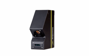

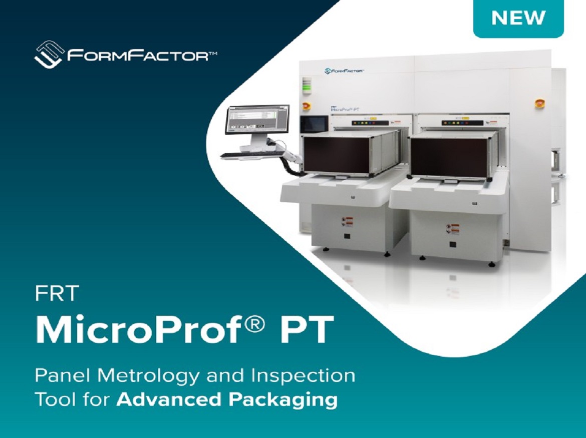
A prominent provider of semiconductor test and measurement equipment, FormFactor, Inc. (NASDAQ: FORM), unveiled the FRT MicroProf® PT today. It is a new semiconductor metrology and inspection tool for rectangular panels up to 600mm that holds 4-5X more dies than a 300mm wafer. A single system can carry out a variety of 3D measurements and defect detection on large format panels with complete automation and hybrid metrology capabilities, facilitating heterogeneous integration of chipsets used in cutting-edge packaging technologies like fan-out panel-level packaging (FoPLP).
Using connection components like micro bumps, TSVs (through-silicon vias), and interposers, FoPLP and other advanced package techniques stack many semiconductors dies into a single heterogeneous package. In order to evaluate the form of these inter-die connections as well as the thickness, roughness, and other properties of the film and metal layers that make up each device, the new MicroProf PT with SurfaceSensTM technology incorporates a number of high-precision sensor options. The instrument can also give vital defect inspection data for process management and yield enhancement, fully integrating into factory floor automation via SECS/GEM protocols.
The MicroProf PT is the newest member of FormFactor’s Advanced Packaging metrology product family, joining the company’s well-known MicroProf AP wafer-level packaging solution. Its salient characteristics are as follows:
- Metrology and defect inspection applications in one tool
- Full automation with two loaders for panel FOUPs, for panels up to 600mm x 600mm
- Multi-sensor setup including topography, field-of-view, and film thickness with hybrid software evaluation to evaluate highly complex structures
- Film thickness measurements from micron-range down to tens of nanometers
- Wide range of handling capability – from substrates a few millimeters thick to 200µm, including organic and glass
Large-format panel substrates offer a significant cost-reduction trajectory, according to Thomas Fries, vice president, and general manager of FormFactor’s Emerging Growth Business Unit. “Innovation in advanced packaging is rapidly advancing process capability,” he added. The ability to design and produce these new processes on affordable panels is provided by the multi-sensor MicroProf PT to our customers.
Credits: FormFactor
Click on the following link Metrologically Speaking to read more such news about the Metrology Industry.