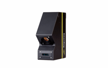

Nearfield Instruments B.V., a supplier of weighty cycle control metrology answers for cutting-edge semiconductor gadgets, today sent off AUDIRA™ – the business’ solitary in-line, non-horrendous subsurface metrology framework for cutting-edge semiconductor producing. The AUDIRA framework gives profoundly exact and reproducible nanometer-level estimations of covered elements and deformities, like voids, in cutting-edge memory and rationale gadgets.
“AUDIRA is a distinct advantage for cutting edge semiconductor producing. It gives estimation information that was already not accessible without eliminating the wafer from the line,” said Hamed Sadeghian, President, of Nearfield Instruments. ” Most importantly, the AUDIRA provides process engineers with insight into the wafer’s innermost layers, which they had never previously been able to measure non-destructively or even knew to look for. AUDIRA, similar to our most memorable item QUADRA™, transforms in-line metrology and examination into an additional worth in the semiconductor-producing process.”
Nearfield Instruments guesses that AUDIRA will supplement transmission electron microscopy (TEM) and basic aspect examining electron microscopy (Cd SEM) for subsurface interaction control estimations. With the added benefit of being in line with a quick turnaround time, AUDIRA employs an acoustic method that is swift, extremely precise, and non-destructive.
Nearfield Instruments combines its own proprietary atomic force microscopy (AFM) technology with an acoustic microscopy method with AUDIRA. The AFM test is utilized to ‘pay attention’ to the sound waves getting through the wafer layers. The wave reflects information back after interacting with all of the device’s transitions and surfaces. The example of that reflected wave and the hour of appearance contains information about the design beneath the surface. With steps as small as a few tenths of a nanometer, the AUDIRA scans the die. After that, the data are turned into a comprehensive pattern of the underlying layers, which can be used to measure features in the subsurface.
AUDIRA is additionally significant for estimating shallow highlights through the surface. Utilizing the AFM test, surface versatility varieties can be immediately estimated to uncover insights regarding the design underneath. Nearfield Instruments works with clients to foster a recipe for when to utilize acoustics and at what recurrence, for which layers neighborhood versatility estimations are ideal, and when to change to wave proliferation plans.
The QUADRATM surface metrology solution is also part of the Nearfield Instruments product line. It includes a noteworthy multi-scaled down AFM head engineering joined with feedforward direction organizer (FFTP) imaging innovation to empower on-gadget, non-horrendous estimations for in-line process observing of extremely high-viewpoint proportion structures as well as crossover holding and EUV oppose basic aspect metrology. QUADRA has shown an element of more than 100x improvement in imaging obtaining time when benchmarked against existing cutting-edge AFM frameworks.
Orders for AUDIRA can be placed right now, and the first systems will be delivered to world-class semiconductor fabs in Q2 2024.
Click on the following link Metrologically Speaking to read more such news about the Metrology Industry.