Atomic force microscopy is playing a bigger role as critical dimensions shrink and more chips are assembled in packages; competition is growing.
Competition is heating up in the atomic force microscopy (AFM) market, where several vendors are shipping new AFM systems that address various metrology challenges in packaging, semiconductors and other fields.
AFM, a small but growing field that has been under the radar, involves a standalone system that provides surface measurements on structures down to the angstrom level. (1 angstrom = 0.1nm.) AFMs are versatile, but they are relatively slow and sometimes relegated to select applications. The latest AFMs are faster and have broader capabilities, which could extend the reach of the technology and possibly alter the metrology landscape.
Developed in the 1980s, AFMs are one of several different systems used in the field of metrology, which is the art of measuring structures. Used in the lab and fab, AFMs are found in life sciences, semiconductors and other fields. Basically, an AFM system incorporates a cantilever with a tiny hard tip or needle. In operation, the tip scans the surface of a structure, providing three-dimensional measurements with resolutions from 100µm to 0.1nm.

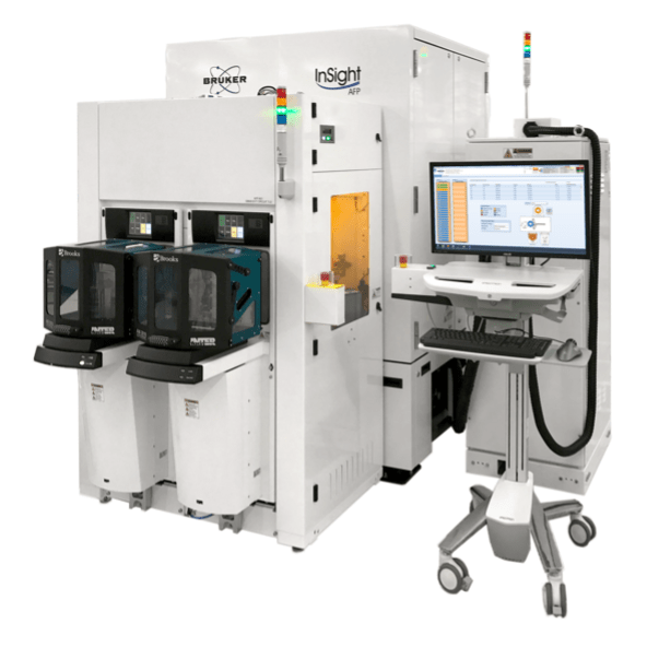
Fig. 1: AFM metrology system. Source: Bruker
AFMs are complementary to other metrology tool types, and can handle some but not all of the measurement requirements in fabs. In fact, no one metrology tool can handle all of the demanding measurement requirements for today’s complex III-V, logic and memory devices. In logic fabs, for example, chipmakers rely on several metrology tool types to measure complex materials and structures in devices. AFMs are used in select parts of the process. Generally, other metrology tool types, namely optical-based systems, provide a larger percentage of the CD measurements in fabs, simply because they are more mature and faster than AFMs.
AFMs have some throughput and other limitations. It’s difficult to make an AFM tip small enough to handle narrow-trench mode measurements. In response, AFM vendors are making advancements in these areas. Even then, they won’t displace the other metrology tools. Nonetheless, AFMs have evolved and become a valuable tool in the metrology toolbox.
“In the early days, it wasn’t mainstream. AFMs required a lot of knowledge and a trained operator,” said Ingo Schmitz, a product marketing engineer at Bruker. “AFMs transitioned into something that has become more mainstream. I say this because of the type of customers that we see. Before, it was early adopters. Today, it’s not the middle of the curve, but it’s almost everybody. They see distinct advantages using it. We’re pretty much in almost every fab. It’s only growing.”
Along with this shift, competition is intensifying:
- Bruker, Park Systems, and others are shipping new AFMs.
- Two newcomers, Nearfield Instruments and Infinitesima, are developing fast versions of the technology.
- New AFM applications are emerging, such as EUV resist characterization, gate-all-around transistors, and hybrid bonding for packaging, among others.
AFM landscape
At last count, more than a dozen suppliers compete in the AFM market, which in total is roughly a $200 million business, analysts said. Bruker, Oxford, and Park Systems are the larger AFM suppliers. Most are smaller players with lab tools. And two newcomers — Nearfield and Infinitesima — have joined the field.
Vendors sell R&D and/or production tools with different features. In one example, Park Systems recently rolled out a new AFM, which autonomously executes all set up and scanning processes. In addition, Bruker and others are adding new capabilities to their AFMs.
AFMs are found in labs, as well as the offline and in-line production flows in fabs. An AFM consists of a control computer, detector, laser, and a cantilever with a tiny probe or tip. Based on carbon and silicon materials, the hard tip come in different shapes and sizes at the nanometer scale.
In operation, the tiny tip scans the surface of a sample along one row and then moves to the next row in a raster scan motion. It conducts measurements on surfaces using tip-sample forces. The cantilever deflection is measured, which generates a 3D map of the surface topography.
“On one end of the scale, you are able to resolve atomic and molecular lattices,” Bruker’s Schmitz said. “If you go to the other end, you can go up to about 60μm to 100μm square.”
AFMs are used in many applications. “In general, AFM is a non-destructive inspection technique. With a lot of optical tools, there’s a lot of modeling. With AFM, it’s a direct measurement,” said Stefan Kaemmer, president of Park Systems. “If you look at the pure applications for AFM, there are basically three. It’s surface roughness measurements. The second one is step heights. And the third one is angles. There are other things you can do with an AFM. On the failure analysis side, you can combine that with electrical measurements. Electrical fault isolation is an example. You could do scanning capacitance, and look at doping profiles.”
AFMs also are used for defect analysis and review on wafers. “Basically, the defects need to be reviewed to enable process engineers to conduct root cause analysis for troubleshooting yield excursions. And for that, the size and shape of these defects provides critical information. This is where AFM fits in. We can do a non-destructive review of these defects,” Kaemmer said.
Then, there are various hybrid tools. For example, an AFM can be combined with infrared spectroscopy (AFM-IR) for chemical analysis.
AFMs have gained the most traction in various post processing steps, especially etch and chemical-mechanical-polishing (CMP). In a fab flow, materials are deposited on wafers. The excess materials are removed and the surface is planarized using a CMP system. At times, the CMP process may cause unwanted erosion or dishing effects on the surface. In the post-CMP process, AFMs conduct surface roughness measurements at the angstrom level.
However, the technology faces some challenges. For one thing, AFMs are slow compared to other tools. In addition, while the tiny tips within the AFM system are capable of conducting measurements inside trenches in structures, it’s difficult to develop small enough tips for the smallest trenches.
“Imagine trying to measure the sidewall topography in a FEOL (front-end-of-the-line) high-aspect ratio structure, such as the sidewall of a deep and narrow crater, with the tip of a physical needle,” said Paul van der Heide, director of materials and component analysis at Imec. “AFM is a scaled down version of this. And this becomes more difficult when there is selective etch back of specific layers within the crater. No matter how small the needle is, both geometric issues and tip adhesion are becoming more of a concern, especially if the needle is to be brought in at an angle with respect to the wafer surface. And one also needs to ensure the needle remains sufficiently robust, as a floppy needle will further exacerbate adhesion issues. But that being said, there are always interesting ideas being developed for AFMs.”
AFMs are getting faster, too. Bruker sells a 300mm AFM tool designed for post-CMP profiling and etch metrology for advanced nodes. Throughputs are greater than 300 sites per hour, or more than 30 wafers an hour.
There are other ways to speed up AFMs, as well. Traditional tools consist of one AFM head. In contrast, Nearfield is developing a tool with four AFM heads, which boosts the throughputs. Nearfield’s tool also has a new imaging mode, which performs measurements in deep and narrow trenches.
Meanwhile, Infinitesima has developed a Rapid Probe Microscope (RPM), a high-speed version of the technology. “As semiconductor processes continue to scale, metrology and inspection are not keeping up with the needs of advanced processes,” said Peter Jenkins, president and CEO of Infinitesima. “There is a need for metrology in the third dimension. AFM is good in that aspect, but traditional AFMs are slow, taking minutes to capture an image. The probe lifetime is the other main challenge with a probe-based metrology system. Infinitesima has pioneered a 3D metrology probe technology that is different from a classical AFM. What sets us apart is that we’ve integrated an interferometer system to measure the exact position of the probe in three axes. Photo-thermal activation of the probe enables us to operate 100 times faster than a classical AFM system and measure topography without the traditional probe lifetime issues.”
RPM is targeted for various applications. First, Zeiss has integrated an RPM module in its mask repair tools to validate repairs. Second, Infinitesima and Imec are working on 3D tomography using RFM. Third, Infinitesima is developing a standalone metrology system.
Where AFMs fit in logic
Time will tell whether the new systems will change the AFM landscape. Nonetheless, AFMs in general will play a role in the development of devices.
Manufacturing chips of all types is a challenging process. A given device undergoes a multitude of process steps using various equipment in a fab. A mishap could occur at each step, causing defects and/or variations in chips.
So in fabs, devices are inspected for defects using inspection systems. Chip structures are measured using metrology tools to ensure they meet spec.
There are different types of metrology systems, which are subdivided into various categories, such as dimensional, compositional, and others. The compositional segment involves metrology systems that conduct film thickness measurements.
AFMs, CD-SEMs, optical CD (OCD), and other tools fall under the dimensional metrology category, which take the CD measurements of structures, such as height, length, and width.
A critical-dimension scanning electron microscope (CD-SEM) takes top-down measurements. Using polarized light, OCD involves a tool that performs CD and film measurements. OCD uses a measurement technique called scatterometry, which characterizes the properties of samples.
Each chip type has different metrology requirements. Take logic, for example. For years, leading-edge logic chips, such as microprocessors, were based on traditional planer transistors. A chip incorporates a multitude of transistors, which operate like a switch in devices.
At 28nm and above, planar transistor structures consist of larger features. For planar transistors, metrology is a straightforward process. Chipmakers use a handful of metrology systems here, namely CD-SEMs and optical tools. AFM is used in post-CMP and etch applications.
“The key steps in legacy nodes are managed mostly through thin-film metrology to measure the deposition, etch, and CMP steps, and with CD-SEMs for dimensional control,” said Kevin Heidrich, senior vice president at Onto Innovation. “There is some adoption of OCD metrology for trench, spacer sidewall, and other simple 3D applications.”
At 20nm, the semiconductor world changed when planar transistors ran out of steam. Starting a decade ago, the industry migrated to finFETs, a next-generation transistor. In finFETs, the control of the current is accomplished by implementing a gate on each of the three sides of a fin.
FinFETs enabled the industry to migrate to the next nodes. But finFETs are also harder to manufacture and characterize in fabs. FinFETs consist of tiny three-dimensional structures and complex materials, which are difficult to measure.
That explains why finFETs require more than a dozen different metrology systems, including AFMs, CD-SEMs, OCD, and X-ray, among others.
For many CD measurements, chipmakers tend to use OCD. “In the move to finFETs, height, sidewall, and other dimensions became increasingly important,” Onto’s Heidrich said. “That drove significant adoption of OCD.”
For finFETs, AFM traditionally is used to map the erosion and dishing effects of CMP. There are other possible apps. In a paper, Bruker and GlobalFoundries have demonstrated the ability to perform fin height and gate profile measurements using it.
Nonetheless, finFETs will run out of steam after the 3nm node. So starting at the 3nm node in 2022, some chipmakers will migrate to a next-generation transistor type called gate-all-around (GAA). GAA provides more performance with less leakage, because the control of the current is accomplished on four sides of the structure.

Fig. 2: Planar transistors vs. finFETs vs. gate-all-around Source: Lam Research
GAA also involves several challenges. “With finFETs, we had to learn how to perform semiconductor processing on sidewalls better than we had previously, but we could still pretty much see everything we were doing,” said David Fried, vice president of computational products at Lam Research. “In gate-all-around nanosheets/nanowires, we have to do processing underneath the structure where we can’t see, and where it’s much more challenging to measure. And that’s going to be a much more difficult transition.”
For GAA, chipmakers will require the same types of metrology tools used for finFETs. Each tool will have a place in the flow. For example, OCD will provide several CD measurements. Some measurements are harder than others.
“Although there are a number of challenges when developing a process flow for new architectures, one of the more critical in GAA structures will be the inner spacer etch back. This process ensures just the right amount of etch has been applied to release the nanosheets,” Imec’s van der Heide said. “Two non-destructive in-line metrology developments of interest to the industry in this area are scatterometry (Mueller matrix spectroscopic ellipsometry) and Raman spectroscopy, with a priori validation provided through destructive TEM cross-sectional analysis.”
AFMs also will have a place in GAA. “One of the prime examples is ensuring CMP is carried out to the right degree,” van der Heide said. “Too little and the surface remains too rough, and too much and the film being polished may be completely removed. Here, AFM has been the workhorse in the industry dating back to planar structures, and will continue to do so for the foreseeable future.”
For GAA and other devices, AFM suppliers hope to expand the reach with the technology. Using AFMs for GAA, for example, IBM and Bruker demonstrated the ability to characterize multiple structures after the epitaxial growth process and along sidewalls.
For AFM, though, the big challenge is narrow-trench applications in GAA and other devices. Startup Nearfield is developing a solution here.
“We have overcome the limitations of traditional AFMs for measuring narrow and deep trenches,” said Hamed Sadeghian, CEO of Nearfield. “This is achieved via a feed-forward trajectory planner (FFTP) mode. FFTP measures high-aspect ratio structures, where the space of trench or hole diameter is less than 20 to 40nm and the depth is about 200nm. This mode controls the motion of the probe to such an extent that it minimizes the interaction with sidewalls and ensures it reaches the bottom of such complex structures.”
For finFETs, Nearfield’s tool handles 3D profiles. In GAA, the system is designed to measure lateral recesses and deposition.
Other solutions are in the works. Bruker’s AFMs address ~4:1 aspect ratios, measuring features 12nm wide x 40nm deep. “In our probe and mode development, we’re supporting GAA metrology development with ongoing testing on EUV resist for 20nm, 16nm, and 12nm CD x 30nm depth to characterize line-top loss, line-top roughness, and profile information,” Bruker’s Schmitz said. “In addition, we’re characterizing STI depth where ~8:1 aspect ratios are typical. The next steps in AFM probe technology will evolve to single-wall carbon nanotube probes with a radius of 1nm to measure 3nm structures for in-line metrology.”
Metrology for advanced packaging
AFMs, meanwhile, also play a role in advanced packaging. In advanced packaging, the idea is to assemble and stack complex dies in an IC package, creating a system-level design.
For some time, packaging houses have shipped various advanced package types, such as 2.5D/3D technologies, fan-out, and others.
Advanced packages address several challenges. For example, in systems, data moves back and forth between a separate processor and memory devices. But at times this exchange adds latency and increases energy consumption. One way to solve the problem is to bring the memory and processor closer together and integrate them in a package.
There are other examples. At each generation, IC vendors integrate more functions on a chip, but this approach is becoming more difficult and costly.
One way to solve the problem is by breaking up the chip into several smaller dies or chiplets, and then assemble them in a package. This concept, called chiplets, is supposed to reduce the cost in developing a system-level design.
“Therefore, the system can be optimized by using the best processor components with an optimum performance/cost process node,” said Xiao Liu, senior program manager from Brewer Science.
Meanwhile, each package type is manufactured using a different process. In some cases, dies are stacked and connected in a package. For this, tiny copper microbumps are formed on the top of the dies.
Then, using a wafer bonder, the bumped dies are connected with one another and bonded within a package. Bumps and pillars provide small, fast electrical connections between different devices in the package.
The most advanced microbumps are tiny structures with a 40μm pitch. Using existing equipment, the industry can scale the bump pitches down to 10μm. Then, the industry needs a new technology, namely copper hybrid bonding.
Targeted for 10μm pitches and below, hybrid bonding connects dies in packages using tiny copper-to-copper connections, as opposed to bumps. Hybrid bonding provides more interconnect density, enabling a new class of 3D-like chip architectures.
But hybrid bonding presents some manufacturing challenges in the fab. “The big challenges are wafer surface cleanliness, wafer warpage, and step height between the copper and dielectric materials in a die,” said Tony Lin, technology director at UMC.
In the hybrid bonding flow, the first step is to process chips on a wafer. On the bottom of the wafer, copper bond pads are formed using various process steps. Then, the bond pads on the wafer are planarized using a CMP tool.
Then, the chips on the wafer undergo an activation step. The process is repeated with another wafer.
Using a wafer bonder, the two wafers with the copper pads exposed are bonded using a two-step process. It’s a dielectric-to-dielectric bond, followed by a metal-to-metal connection.
The CMP process is critical here. If the wafer is overpolished, the surface is prone to erosion, and the pads may fail to bond. If underpolished, copper residues can create electrical shorts.
That’s where AFM fits. The tool measures and characterizes the surface topography and bond pads after the CMP process, which is critical.
“You’re not talking about a single pad. By definition, that single pad size is not challenging for an AFM. It’s important to understand the roughness of that pad and then that surrounding area or those transitions from one material to the other. You need to understand those slopes. If you don’t have an accurate AFM, you’re not going to get the right information,” said Hector Lara, director and business manager at Bruker. “Now, you’re looking at multiple pads matching. It’s not just in the physical location in ‘X’ and ‘Y,’ but also in the tilt of those pads. If they’re not going to match, and if your metrology system doesn’t have the ability to have a low out-of-plane motion, then it’s not going to detect those mismatches and angles. And then the bonding will not be as effective or will fail all together.”
Hybrid bonding involves other metrology steps, as well.

Fig. 3: Hybrid bonding flow. Source: Leti

Fig. 4: Die-to-wafer, die-to-wafer hybrid bonding flows. Source: Leti
Conclusion
AFMs are also used in memory, and they are used to characterize the optics in virtual reality systems. Life sciences is a big market for AFMs.
AFM is a key tool in the metrology toolbox, but these systems can’t do it alone. The industry requires other metrology types to ensure successful product ramps.


