• Collaboration to accelerate learning, develop novel methods, and prove new metrology equipment, methods, algorithms, and software Applied Materials, Inc., the leader in materials engineering solutions, and the Fraunhofer Institute for Photonic Microsystems IPMS, Germany’s leading advanced 300mm semiconductor research center, today announced a landmark collaboration to create Europe’s largest technology hub for semiconductor metrology and process analysis. The new hub will provide state-of-the-art metrology systems to accelerate semiconductor research and enhance development projects with chipmakers and the ecosystem.
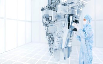
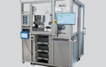
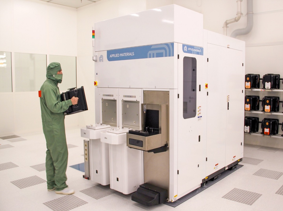
To be situated at the Middle Nanoelectronic Advances (CNT) of Fraunhofer IPMS in Dresden, the innovation center is arranged in the core of Silicon Saxony, Europe’s biggest semiconductor group. The center will be outfitted with Applied Materials’ cutting-edge eBeam metrology gear, including its VeritySEM® Album SEM (basic aspect filtering electron magnifying lens) frameworks, and staffed by Applied engineers and Research and development specialists.
“Fraunhofer IPMS and its accomplices will profit from admittance to Applied’s industry-driving eBeam metrology frameworks”, said Dr. Benjamin Uhlig-Lilienthal, Head of Specialty Unit Cutting edge Registering at Fraunhofer IPMS. ” With Fraunhofer IPMS’s unique capability to loop wafers directly with semiconductor manufacturers, the new technology hub will provide advanced wafer-level metrology in our industrial CMOS environment.
“Our cooperative metrology center will speed up learning cycles and the advancement of new applications for the Fraunhofer Establishment, Applied Materials, and our clients and accomplices in Europe,” said James Robson, Corporate VP for Applied Materials Europe. ” This special innovation center point will have the capacity to test and qualify processes on various substrate materials and wafer thicknesses basic to applications across the different European semiconductor scene.”
Metrology is essential in the development of microprocessors as the need might have arisen to exactly screen and control the nature of individual semiconductor fabricating steps and successions. Chipmakers use metrology gear at basic focuses to assist with approving physical and electrical qualities and keep up with target yields.
Click on the following link Metrologically Speaking to read more such news about the Metrology Industry.