
- New VeritySEM® 10 system delivers industry-leading resolution and imaging speed to help chipmakers accelerate process development and maximize yield in high-volume manufacturing
In order to properly measure the key dimensions of semiconductor device features patterned with EUV and the nascent High-NA EUV lithography, Applied Materials, Inc. today unveiled a new eBeam metrology system.
After a lithography scanner transmits patterns from a mask to a photoresist, chipmakers employ CD-SEMs (critical dimension scanning electron microscopes) to collect sub-nanometer measurements of the patterns. To make sure the patterns are accurate before they are etched into the wafer, these measurements continuously calibrate the performance of the lithography process. After etch, CD-SEMs are also utilized to compare the desired patterns to the outcomes on the wafer. By enabling a feedback loop between lithography and etch and aiding in process control, CD-SEMs provide engineers with highly correlated data sets for comprehensive process adjustment.
The crucial dimensions of semiconductor device features are more difficult to measure as photoresists become thinner under EUV, particularly under High-NA EUV. The CD-SEM must be able to precisely apply a narrow eBeam to the little area occupied by the incredibly thin photoresist in order to take high-resolution pictures that offer exact, sub-nanometer measurements. Photoresists and eBeam energy interact, and if the landing energy is too high, the resist will shrink, causing mistakes in the pattern and distortion of the resist. Conventional CD-SEMs are unable to produce beams that are both narrow enough and low energy enough to minimize interactions with the fragile High-NA photoresist.
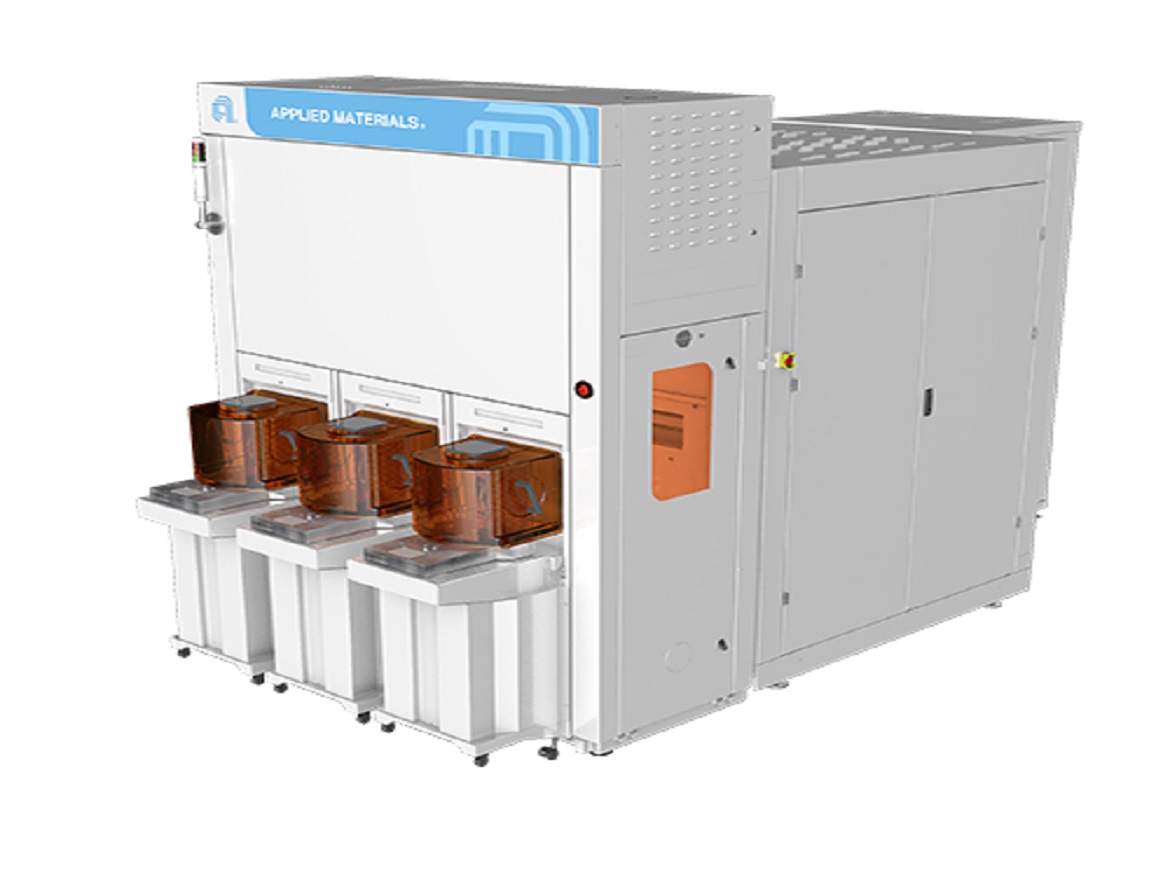
Introducing the VeritySEM® 10 CD-SEM Metrology System
The new VeritySEM 10 device from Applied has a distinctive architecture that allows for reduced landing energy at a 2X improvement in resolution over traditional CD-SEMs. Additionally, it offers a 30% quicker scan rate to further minimize contact with the photoresist and boost throughput. Because of the system’s industry-leading resolution and scan rate, EUV and High-NA EUV lithography and etch processes can be controlled better, enabling chipmakers to create new processes more quickly and increase yield in high-volume production.
Chipmakers are also using the VeritySEM 10 system for key dimension metrology applications in 3D designs, such as 3D NAND memories and Gate-All-Around (GAA) logic transistors, where the system’s backscattered electrons allow for high-resolution imaging of complex structures. The VeritySEM 10 is being used to measure and characterize the selective epitaxy process, which is essential to transistor performance, among other uses for GAA devices. The technology offers a wide field of vision and deep depth of focus for 3D NAND memories, allowing measurements of whole staircase connection architectures and assistance in fine-tuning etch process recipes.
According to Keith Wells, Group Vice President of Imaging and Process Control at Applied Materials, “The VeritySEM 10 system is a breakthrough in CD-SEM technology that resolves the metrology challenges of major technological inflections that will shape the industry in the years ahead.” “The system’s unique combination of low landing energy, high resolution, and faster imaging speed helps pave the way to High-NA EUV, Gate-All-Around transistors, and high-density 3D NAND.”
With more than 30 systems supplied over the past year, the VeritySEM 10 system is generating substantial commercial interest from top logic and memory clients. The system has been chosen by numerous clients to be the official development tool for GAA transistors. The system has been chosen as the development and process tool of record by all major 3D NAND customers, and it has also been chosen by a number of DRAM customers.
The VeritySEM 10 system from Applied will be covered in more detail at the company’s upcoming “New Ways to Shrink: Advanced Patterning Products Launch” event.
Credits: Applied Materials
Click on the following link, Metrologically Speaking to read more such news about the Metrology Industry.