The semiconductor industry is an important strategic pillar for the economy in Germany and the innovative strength of ZEISS has been vital to this. Baden-Württemberg’s Governor, Winfried Kretschmann, saw this firsthand during his visit to the ZEISS site in Oberkochen.
Oberkochen, Germany | June 2022 | ZEISS Group
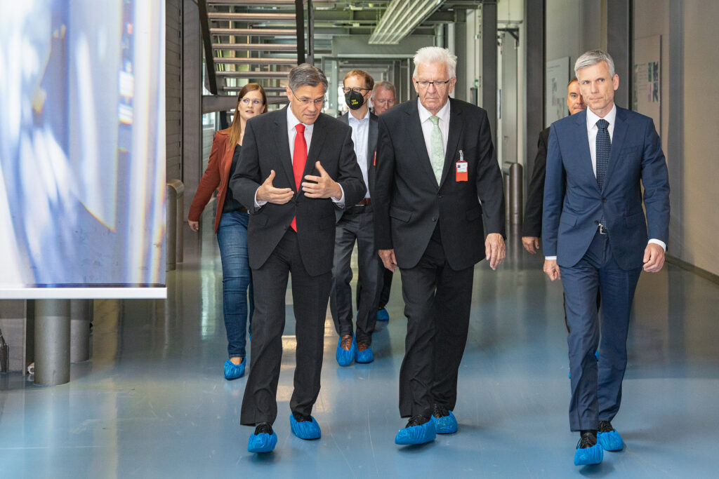
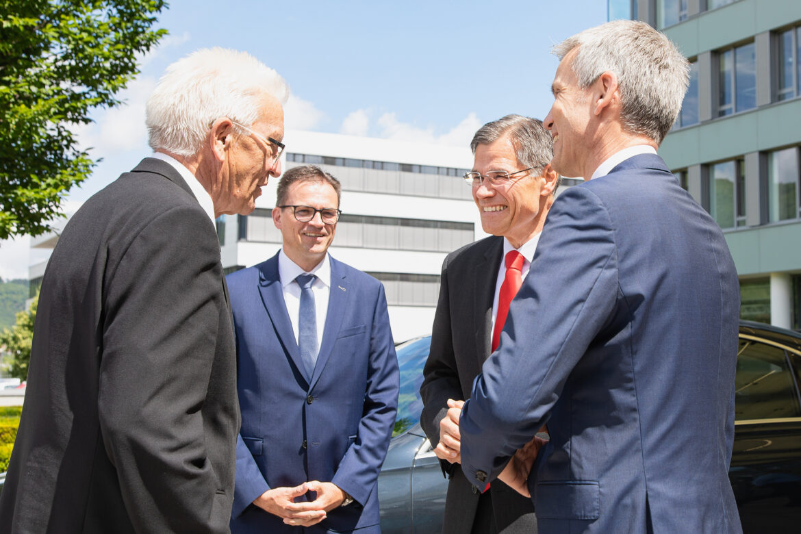
The Governor of the state of Baden-Württemberg, Winfried Kretschmann, visited the Oberkochen headquarters of ZEISS, an internationally leading technology enterprise operating in the fields of optics and optoelectronics. Dr. Karl Lamprecht, President and CEO of ZEISS and Andreas Pecher, Member of the ZEISS Executive Board with responsibility for the Semiconductor Manufacturing Technology (SMT) segment, gave the Minister President not only a glimpse into the production of the “most precise” mirrors in the world, but also impressed him with the innovation and investment power of the company based in the Ostalb region.
The heart of digitalization starts beating in a clean room in Oberkochen
The ZEISS Semiconductor Manufacturing Technology (SMT) segment covers important key processes in the production of microchips. Together with its Dutch partner ASML, ZEISS is the world’s only manufacturer of EUV lithography machines for chip production. Optics is the key element to such appliances and ZEISS develops and manufactures them in Oberkochen.
While touring the clean rooms where the innovative extreme ultraviolet (EUV) lithography systems are produced, Governor Kretschmann and his delegation were impressed by the complexity and precision of the technologies and the processes used to manufacture them.
Since EUV light is absorbed by all materials, even air, ZEISS has developed an optical system made up entirely of mirrors, which operates in a high vacuum. The requirements for the EUV mirrors and thus their manufacture and measurement are extreme: they must be produced and coated with atomic precision. This level of precision requires extremely accurate measuring technology, the mirrors for the latest optic are measured in vacuum chambers five meters in diameter, and it takes more than a year to produce one of these mirrors.
“Gaining insights into the heart of ZEISS was a truly memorable experience. The EUV technology developed here is what makes digitalization possible in the first place, today and in the future,” emphasized Governor Kretschmann during his visit. “ZEISS makes an enormous contribution with its research and development to enabling autonomous driving, the new wireless standard 5G, artificial intelligence and other future innovations.” Kretschmann said that the company has been a pioneer in the production of state-of-the-art microchips globally: “We can be pleased to have such an innovative company in our federal state. As a business location, Baden-Württemberg needs joint research projects and innovation drivers to remain competitive and to be able to play a leading role in the future.
The tour also offered an opportunity to discuss the role of the semiconductor industry as an important strategic pillar for the economy in Germany and Europe. The industry, with a high level of innovative strength, contributes significantly to Germany as a high-tech location and shows a tremendous growth dynamic.
Strong prospects with future-oriented technologies
“Our innovation strength is paramount to the success of ZEISS’ dynamic growth. Our EUV Technology is such a good example of this. On the one hand, it alone facilitates advancement for digitalization and progress through digitalization on the other. “At the same time technology also improves energy efficiency with its high performance and consequently contributes to sustainability,” said Lamprecht during the tour.
ZEISS and ASML have been developing the next generation of EUV for some time: an optical system with a numerical aperture of 0.55, known as a High-NA EUV optic. This technology will allow semiconductor manufacturers to produce more powerful and more energy-efficient chips at lower costs in future.
“Future-oriented technologies require investments alongside innovative strength. The development of EUV technology was a marathon – and a success resulting from European cooperation and joint research,” added Pecher. “The development of the next EUV generation, High-NA EUV, shows that we are not resting on our laurels.”
Large-scale investment is once again required for this purpose. We are hoping for a positive sign at federal level as regards research funding and support with implementing the necessary infrastructure.”
Technological progress for the growth fields of tomorrow
ZEISS has a turbulent history of 175 years characterized by technical milestones. They serve as a testament to an ongoing desire to innovate and the pursuit of technological progress – innovations are the lifeblood of ZEISS. ZEISS technologies shape fields such as medicine, the life sciences, and the automotive industry, as well as information technology and communications. The technology leader achieved this by demonstrating once again how it is possible to successfully challenge the limits of what is technically feasible through innovations.
The ZEISS strategy is globally aligned with long-term megatrends such as digitalization, demographic change, and new mobility patterns.
Choosing this strategy during the current challenging geopolitical conditions was the right course of action and the excellent start to 2021/22 backs this up.
Press Contact
Jörg Nitschke
Head of Corporate Brand and Communications
ZEISS Group
Phone: +49 7364 20-3242
joerg.nitschke@zeiss.com
About ZEISS
ZEISS is an internationally leading technology enterprise operating in the fields of optics and optoelectronics. In the previous fiscal year, the ZEISS Group generated annual revenue totaling 7.5 billion euros in its four segments Semiconductor Manufacturing Technology, Industrial Quality & Research, Medical Technology and Consumer Markets (status: 30 September 2021).
For its customers, ZEISS develops, produces and distributes highly innovative solutions for industrial metrology and quality assurance, microscopy solutions for the life sciences and materials research, and medical technology solutions for diagnostics and treatment in ophthalmology and microsurgery. The name ZEISS is also synonymous with the world’s leading lithography optics, which are used by the chip industry to manufacture semiconductor components. There is global demand for trendsetting ZEISS brand products such as eyeglass lenses, camera lenses and binoculars.
With a portfolio aligned with future growth areas like digitalization, healthcare and Smart Production and a strong brand, ZEISS is shaping the future of technology and constantly advancing the world of optics and related fields with its solutions. The company’s significant, sustainable investments in research and development lay the foundation for the success and continued expansion of ZEISS’ technology and market leadership. ZEISS invests 13 percent of its revenue in research and development – this high level of expenditure has a long tradition at ZEISS and is also an investment in the future.
With over 35,000 employees, ZEISS is active globally in almost 50 countries with around 30 production sites, 60 sales and service companies and 27 research and development facilities. Founded in 1846 in Jena, the company is headquartered in Oberkochen, Germany. The Carl Zeiss Foundation, one of the largest foundations in Germany committed to the promotion of science, is the sole owner of the holding company, Carl Zeiss AG.
Further information at www.zeiss.com
Semiconductor Manufacturing Technology
With its product portfolio and expertise, the Semiconductor Manufacturing Technology segment of ZEISS covers a variety of key processes in the production of microchips. Its products include semiconductor manufacturing optics – notably lithography optics – as well as photomask systems and process control solutions for semiconductor manufacturing. Thanks to ZEISS technology, microchips are becoming increasingly smaller, more powerful, more energy-efficient and more affordable. The electronic applications of these ongoing enhancements enable global progress in many disciplines such as technology, electronics, communication, entertainment, mobility and energy. Semiconductor Manufacturing Technology is headquartered in Oberkochen. Other sites include Jena, Rossdorf and Wetzlar in Germany, as well as Bar Lev (Israel) and Dublin, CA and Peabody, MA (USA).
