
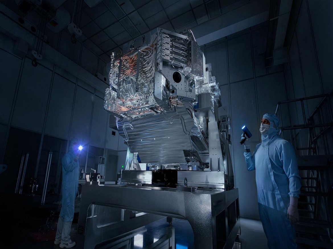
The worldwide unique High-NA-EUV lithography sets new standards for the production of state-of-the-art microchips. ZEISS has developed and manufactured the optical system as the heart of this new technology. The first machine for the High-NA-EUV lithography was recently delivered by the strategic ZEISS partner ASML. The first microchips are set to be produced in series from 2025.
- High-NA-EUV lithography enables a three times higher transistor density on the microchip
- At the heart of the technology is the world’s most precise optical system from ZEISS
- Development of High-NA-EUV lithography builds on a strong European partner network
Oberkochen, Germany | 30 January 2024 | ZEISS Semiconductor Manufacturing Technology
Whether it’s about artificial intelligence, autonomous driving, smart cities or the Internet of Things: the groundbreaking technologies and developments of the future will require enormous computing power – with ever more effective microchips. Together with its strategic partner ASML, the Dutch manufacturer of lithography systems, the ZEISS Semiconductor Manufacturing Technology (SMT) segment has now created the basic prerequisites for the production of integrated circuits at a new level. With the so-called High-NA-EUV lithography, significantly smaller structures can be realized on the carriers of the microchips – the wafers – and thus even more powerful, energy-efficient and cost-effective chips can be produced. The first series production using the new technology is set to begin in 2025.
Driving global digitalization forward
The finest structures, the most precise optics, the most complex measurement technology: “We simply can’t talk about High-NA-EUV lithography without waxing lyrical in superlatives,” declares Andreas Pecher, member of the ZEISS Executive Board and President & Chief Executive Officer of the SMT segment. EUV stands for “extreme ultraviolet” – in other words, extremely ultraviolet light. NA stands for “numerical aperture” and thus for an even larger aperture angle of the ZEISS optics than in the most modern process to date, EUV lithography. While around 1,000 transistors nestled onto a microchip in 1970, this figure exceeds 55 billion today. “High-NA-EUV lithography will enable a three times higher density of transistors on microchips than before – thereby multiplying computing power to an even greater factor,” says Pecher. “Originally formulated by Intel co-founder Gordon Moore and stating that the number of transistors on a microchip doubles approximately every two years, Moore’s Law is clearly set to continue.”
A superlative technology
ZEISS has invested around ten million man-hours in research and development for High-NA-EUV lithography. Strategic partner ASML and many other European partners are also involved in the development of the technology. “We’re always working on pushing the boundaries of what’s technically feasible,” states Pecher. “Our aim is to actively shape digitalization worldwide with our innovations by enabling the chip industry to make new technological leaps. We’ve set ourselves ambitious goals to achieve this. Our perseverance over more than 25 years has now paid off: ASML’s new wafer scanner for the High-NA-EUV lithography is the most modern, complex and precise machine for microchip production in the world – and we’re very proud to provide the optical system as the heart of this machine.”
More light for more details
Microchips are manufactured in wafer scanners using a process known as lithography. Different photomasks are used to expose the different layers of the chip structure layer by layer on the wafer – similar to a slide projector. The optical system from ZEISS is an essential component of the wafer scanner. It contains mirrors that reflect the light and direct it to the right spot with nanometer precision. “Thanks to the larger numerical aperture and the new mirrors for the High-NA-EUV lithography, we can capture more light and thus expose it with even greater detail and precision. Experience has shown that the smaller the chip structures are to be, the larger the optical system consisting of projection optics and illumination system will be,” says Dr. Peter Kürz, Head of the field of business High-NA-EUV lithography at ZEISS SMT. The illumination system for the High-NA-EUV lithography consists of around 25,000 parts and weighs more than six tons. With more than 40,000 parts, the projection optics weigh around twelve tons and ensure high-precision focusing of the light in the wafer scanner. Yet the structures on the finished microchip are only a few nanometers in size. For comparison: one nanometer corresponds to 0.0000001 centimeters. In order to image such structures, the mirrors need to be very precise. To achieve this, more than 100 extremely thin silicon and molybdenum layers are vapor-deposited onto the mirror surface – each layer only a few atomic layers thick. “The precision of the mirrors can be explained with a thought experiment: Imagine a mirror made so big it covers the surface area of Germany. At this size, the largest unevenness would be less than 100 micrometers. That’s 0.01 centimeters – almost as fine as a human hair,” says Kürz.