
Read the latest technical article published in Chip Scale Review.
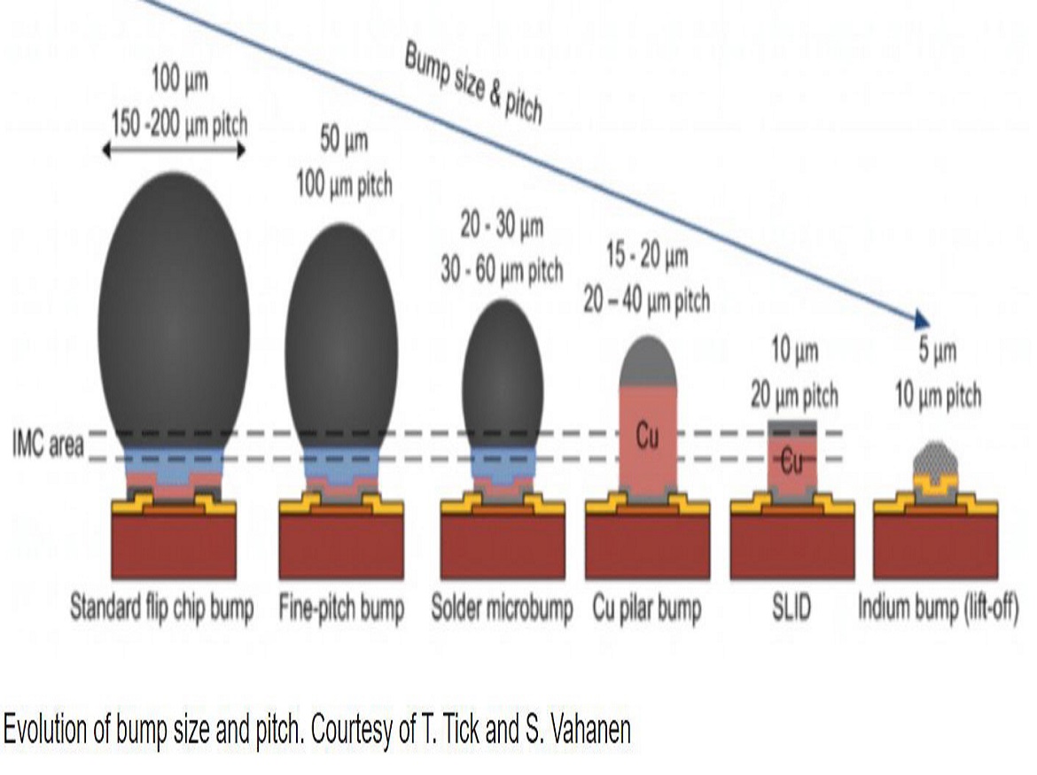
The capacity to process hundreds or thousands of dies simultaneously and the small container size of chip-scale wafer-level packaging (WLP) are also significant advantages. Depending on the application, a range of bump configurations is conceivable, as shown in Figure 1 [1]. Maintaining the homogeneity of copper pillars or solder bumps throughout a 300mm wafer is one challenge with WLP. To guarantee device dependability, metrology and inspection are required. Wafer-level bump height verification, however, is particularly difficult due to decreasing bump heights and spacing as well as high aspect ratios.
Additionally, it is getting more and more important because even slight changes in bump height across a wafer might lower yield. The performance of both thermal and electrical devices can be impacted by bumping flaws [2].
Reducing the number of inspection processes or merely testing a sample of the wafers entering the line can be appealing. Production may accelerate as a result. A partial inspection might be the best course of action for legacy processes where the yield is high. It becomes clear that cutting back on inspection does not result in time savings over the long run when design guidelines change and yield declines. Early defect detection is the best strategy to increase yield, especially for a novel process. This frequently necessitates a complete inspection of every wafer in every batch.
Strict inspection procedures lessen the need to rework or scrap wafers by locating the primary cause of faults.
Speed and location in the process flow are two disadvantages of the current bump height measurement techniques. They hinder production and frequently fail to detect flaws at an early enough stage. 100% inspection is frequently abandoned for high-volume production because to the time needed for testing, even though it is customary throughout process development. Successful metrology and inspection depend on quick, precise measurements. This article compares 3D fringe projection technology to traditional methods for measuring bump height to demonstrate the advantages of using it to evaluate solder bumps and copper pillars at the wafer level.
Conventional bump height measurement
A copper pillar, a nickel barrier layer, and a tin/silver/copper (SAC) solder bump make up pillar bumps. As seen in Figure 2, bump height measurements are normally collected following the last photoresist stripping phase. This happens after the bump’s three levels have all been deposited.
Line scan triangulation is used to assess noncontact bump height traditionally. The object being measured reflects a laser or white light beam that is incident on it. Line scan triangulation involves projecting a line onto the object from the light source. The reflection is recorded and the distance is calculated by a detector made up of several photosensors. An informational map of bump height is created by scanning a wafer. There are two main problems with line scan triangulation. Speed is one of them. Since 100% inspection is not cost-effective, a 300mm wafer may include hundreds of millions of copper micro bumps [3]. Line scan triangulation also has the issue of occurring too late in the production process.
Credits: Cyberoptics
Click on the following link Metrologically Speaking to read more such blogs on Metrology.