
Challenges:
- In semiconductor manufacturing, where devices are extremely sensitive and susceptible to damage from particulate contamination, fine particles can have disastrous effects.
- Particles can still form inside process tools, where they can cause defects and harm yields, despite manufacturers’ best efforts to prevent contamination through air filtering and recirculation methods.
- Rapidly recognizing ‘when’ and ‘where’ airborne particles start is trying with customary strategies.
The three broadly involved techniques for molecule discovery in photolithography conditions — benchtop and handheld molecule counter, screen reticles, and in-situ screen molecule scanners — all have critical downsides.
- Utilizing the benchtop and handheld strategies, arriving at all areas of interest is many times unthinkable.
- Monitor reticle scanning causes long delays in the delivery of test results, and benchtop counters frequently fail to follow the reticle path.
- The conventional method could be used to process product wafers because it is time-consuming and requires the use of a tool.
Solution: In-Line Molecule Sensor™ (IPS™)
- CyberOptics’ In-Line Molecule Sensor resolves these issues, offering an answer educated by a careful comprehension regarding the defilement and discovery issues that cycle designers or administrators face.
- IPS is an expansion of CyberOptics’ Airborne Molecule Sensor™ (APS/APSRQ™) innovation, which has been perceived as the Most popular Strategy (BKM) in fabs around the world.
- IPS can be introduced anyplace in the process chamber exhaust line, where it uses a powerful blue laser to rapidly screen, recognize, and investigate particles down to 0.1µm.
- Molecule sources can be identified ‘when and ‘where’ they happen, consequently decisively further developing instrument uptime and first-pass wafer yields by specifically overhauling the segments of an apparatus causing molecule age.
- Dissimilar to elective items, the IPS works consistently and continuously to convey critical efficiency and money-saving advantages.
- Most observing depends on examination with screen wafers, which are gone through the cycle regularly or because of a pollution issue recognized by downstream review of item wafers. Notwithstanding, because of their discontinuous nature, customary observing techniques frequently miss pollution until harm has proactively been finished and is subsequently identified downstream.
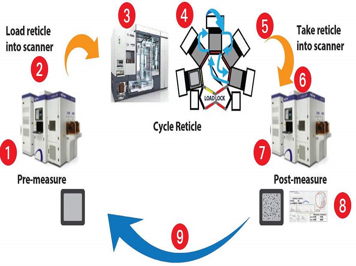
IPS Areas: Supply and Exhaust Lines
- By recording molecule counts versus time, the IPS empowers molecules creating occasions to be associated with process occasions happening inside the device.
- The CyberSpectrumTM software presents instantaneous, average, and accumulated particle count results as well as real-time numerical and graphical particle event data over time. The information is recorded to empower over a significant time span correlation, as well as examination between instruments. Particle adder events and IPS measurements, for instance, have been clearly correlated by EUV customers.
Administrators are saved from the need to open devices to make molecule estimations.
- In addition to CyberSpectrum software, the Software Development Kit (SDK) makes it possible to store recorded data in a network, removing the requirement for a PC specifically designed to store data. Particle data can be analyzed with any software from this central cloud location.
- The IPS from CyberOptics can be used in a wide range of process-sensitive applications, including but not limited to equipment used in controlled environments, vacuum chambers, 3D metal printing equipment, semiconductor process equipment, and EUV processes.
Screen Reticle Filtering Interaction
- Makers confronted consistent disappointment endeavoring to find definitively ‘when’ and ‘where’ airborne particles began while utilizing a loose customary approach.
- Prior to the implementation of CyberOptics’ In-Line Particle SensorTM (IPSTM) technology, it was challenging to manage contamination while simultaneously maintaining production speed.
Summary of Benefits:
- For contamination-free process environments, CyberOptics’ IPS helps producers maximize process yield and tool availability.
- Particle sources can be precisely detected “when” and “where” they form with IPS, wireless wafer, and reticle format sensors, and results can be accessed in real-time and conveniently stored for subsequent analysis.
- Fast outcomes speed recognition of source defilement, shortening support cycles thus. Nonstop checking disposes of personal time and harms to in-advance work, eventually further developing yields while giving huge time and cost-saving advantages.
Click on the following link Metrologically Speaking to read more such case studies about the Metrology Industry.