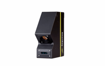

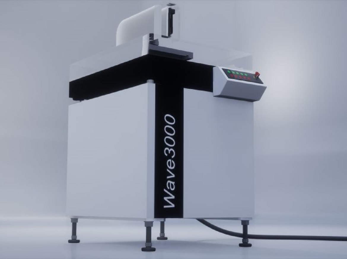
A first-of-its-kind piece of equipment for the measurement and analysis of deformed wafers has been created by ERS Electronic, the global leader in thermal management solutions for semiconductor manufacturing. The Wave3000 can precisely measure wafer abnormalities in specific handling situations, which enables a thorough and accurate examination of wafer warpage, which is essential for guaranteeing the quality of innovative Packaging devices. This is made possible by its innovative optical scanning methodology.
According to Laurent Giai-Miniet, CEO of ERS Electronic, “We see that warpage is becoming an increasingly more complex issue in semiconductor manufacturing with the growing adoption of Advanced Packaging technologies.” It may be brought on by a number of things, including as variations in material qualities, temperature swings, and stress from handling and processing. Wafers that are warped can lead to production problems that result in defects and low yield in addition to process problems.
In order to address this issue, ERS created the Wave3000, a device that can accurately measure and analyze warped wafers from 200 to 300 mm in less than a minute. The system can measure various wafer surfaces and materials, such as silicon, mold compound, and others, thanks to the scanner. By enabling measurements on various platforms, such as pins or an end-effector, its distinctive measurement technology, which is subject to a pending patent, offers versatility.
Following measurement, Wave3000 creates an interactive 3D picture of the wafer that aids in understanding the behavior of the warpage. Users can inspect the warpage profile from any angle while zooming in and rotating the 3D image to determine how it affects the wafer manufacturing process.
“Our new equipment offers a high level of flexibility and precision and can measure warpage, bow, and wafer thickness, which are critical wafer characteristics to avoid yield loss or broken wafers,” explains Debbie-Claire Sanchez, Fan-out Equipment Business Unit Manager at ERS electronic. The cutting-edge Wave3000 software creates a precise 3D image of the wafer surface so the user can assess the influence of warpage on the wafer’s performance and decide with knowing how to optimize process steps for better outcomes.
The company’s portfolio of automatic, semi-automatic, and manual thermal debonding and warpage adjustment tools for Fan-out Wafer-level Packaging is expanded by this innovation. Target customers for Wave3000 include semiconductor manufacturers, OSATs, and research institutions that use advanced packaging methods. This is a very large and expanding market.
Credits: ERS Electronics
Click on the following link Metrologically Speaking to read more such news about the Metrology Industry.