
With Low-Coherence Interferometry
Introduction
Manufacturers in many high-tech industries require precise and reliable indicators of surface quality. Surface inspection is typically carried out in quality control laboratories to measure the surface roughness. Preferably, it should take place right on the production line to provide real-time feedback on a manufacturing or coating process.
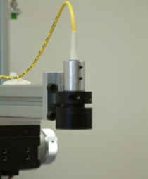
Fiber-based low-coherence profilometers (unlike microscope-like profilometers) are suitable for acquiring surface maps (Figure 1) in both QA labs and production environments. They acquire surface data in long profiles, with micron precision, and at high speeds of 1-30 kHz and faster. Their non-contact probes (Figure 2) inspect from a standoff distance of 30-150 mm and can be positioned far from the profilometer enclosure. In production, they can be mounted on a slide for scanning across a web-based production line. Small and rugged, the probes withstand harsh environments, such as radiation or extremely high or cryogenic temperatures.
For products that are more than a meter wide or long, a single probe or multiple probes can be mounted on an existing X-Y table for measuring surface roughness separately in the X and Y directions.
How Surface Roughness is Measured
A low coherence interferometer is an optical device that splits a beam of broadband light in the infrared range (1300 nm) into two separate beams. One beam is directed at the object surface, and the other at a mirror in the interferometer reference arm. The probe receives and recombines the reflected light from the sample and reference arms and records the resulting interference from which a wide range of information about the object can be retrieved: its surface shape, roughness, and waviness, as well as single or multi-layer coating thickness.
Data Processing
The profilometer processor application software converts optical interference data into high- precision roughness measurements. In the production context, this stream of data is typically forwarded to process control software.
Measuring the Measuring Tape
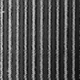
A Mitutoyo roughness gage block (Figure 3) was scanned with a fiber-based profilometer.
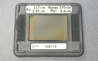
Used as reference pieces, these gage blocks are manufactured so that their micrometer- scale roughness conforms to precise gage maker tolerance grades across their entire surface (Figure 4).
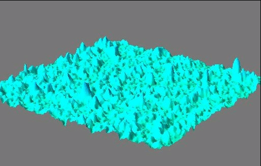
How Rough Does It Get? Characterizing Fuel Cell Surface
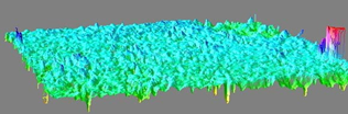
Sample fuel cell plates were scanned and imaged (Figure 6) with the fiber-based profilometer. In addition to calculating the average roughness of the sampled area, other parameters were obtained (Table 1), expressing more precise surface roughness characteristics.
| Roughness indicator | Measurements | |
| Ra | Average roughness | 0.01 mm |
| Rq | Root mean square roughness | 0.01 mm |
| Rsk | Skewness | -0.05 mm |
| Rku | Kurtosis | 13.03 |
| Rv | Maximum profile valley depth | -0.06 mm |
| Rp | Maximum profile peak height | 0.09 mm |
| Rt | Maximum height (distance from highest peak to lowest valley) | 0.16 mm |
Table 1: Fuel cell roughness parameters
Why look beyond Ra?
Average roughness (Ra), a commonly used and well-established roughness parameter, is frequently inadequate for describing the specific character of material roughness. Surfaces with identical Ra’s but dissimilar character may exhibit different properties when it comes to:
- maximizing or minimizing contact with neighboring substance or material
- ability to retain or shed fluids
- ability to resist certain kinds of wear
- ability to resist pressure and stress cracking
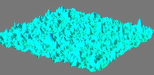
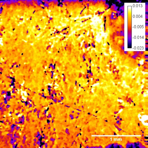
In the case of fuel cells, surface properties impact its efficiency and must therefore be kept between specified target parameters. In addition to imaging the overall roughness of the fuel cell sample (Figure 7), the profilometer roughness application software characterizes the sample waviness and separates waviness from the overall roughness.
Watch your step! Roughness and Shape of Surfaces with High-Aspect-Ratio features: CMP Pads
In the electronics industry, the surface of Chemical Mechanical Polishing (CMP) pads, which are used for smoothing interlevel dielectric layers, is patterned with high aspect channels for guiding abrasive chemical slurry around the polished wafer surface. The surface condition of the CMP pad, including the depth of its channels and the roughness of the surface between them, has a direct effect on the pad’s polishing performance. By measuring actual roughness parameters, technicians in charge of CMP pad monitoring can make the most cost-effective decisions on the timing of pad conditioning or pad replacement.
Too Hot to Handle? Measuring Plasma Coating in Metal Casting
Plasma coating is one of the most versatile methods of altering the surface properties of metal cast elements. In a production environment, metal elements are sprayed with a plasma gun on a continuous basis as they move along a belt at several feet per second. Currently, plasma coating roughness and thickness are inspected in random samples, offline (as in Figure 1).
Fiber-based optical profilometers offer in-process roughness measurement, a significantly more comprehensive and cost-efficient inspection method. A probe is mounted on a slide for scanning across a web-based production line, where it acquires and analyzes the roughness of passing elements in real-time, in both X and Y directions. This results in much faster detection of coating anomalies, more timely correction of system problems, and thus significantly higher savings.
Conclusion
Fiber-based profilometers are ideally suited to surface characterization in both lab and manufacturing environments where high speed and micron precision are required:
- photovoltaic industry: wafer, cell and panel characterization
- semiconductor surfaces
- metal casting, metal plasma coating
- fuel and solar cells
- high-grade glass such as in the optical industry
- multi-layer plastics and films
- high grade (single or multi-layer) polymer tubing
- pitting damage in particle accelerators and explosives labs.
To know more, please check Novacam.