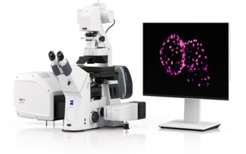

High resolution sensors are supporting improvements in semiconductor metrology and inspection at vital points in the production process. Because the fabrication of semiconductor wafers may require hundreds of steps and weeks of manufacturing time, early-stage defects that go undetected can have costly downstream consequences. Plus, because semiconductor processing always requires a high degree of precision, advances in fabrication methods seem to require ever-finer measurements in a never-ending quest.
Today’s metrology instruments are incorporating high resolution sensors for automated wafer inspection. Resolution, the smallest measurement that a sensor can reliably indicate, may be given in dimensional units such as nanometers (nm) or micrometers (microns). The advantage of using a dimensional unit instead of volts or percent of scale is that it indicates the smallest displacement measurement a sensor can provide. Displacement, a vector whose length is the shortest distance from the initial to the final position of a point undergoing motion, quantifies both distance and direction.
High Precision with Cost Efficiency
Although photolithography tools cost many millions of dollars, the semiconductor industry still wants measurement solutions that combine high precision with cost efficiency. Capacitive probes cost significantly less than laser interferometers while matching or exceeding them in terms of stability, precision, and resolution. As trends like smaller gaps, higher yields, digital amplifiers, and 3D ICs become more common, capacitance-based solutions will be used ever more widely in semiconductor metrology and inspection.
Smaller Gaps and Micron Accuracy with Thermal Stability
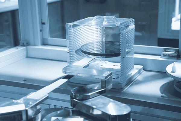
Photolithography, a microfabrication process that transfers a geometric pattern onto a substrate, needs to account for smaller and smaller gaps between lines. To obtain IC line widths as small as 7 nm, high resolution is critical. Without adequate heat dissipation, however, adverse effects from temperature gradients may occur. As this application note explains, a modular capacitance system can achieve dynamic measurement accuracies of 0.1 nm (.0001 microns) while using the existing power supply for lower power consumption and greater thermal stability.
Increased Yields, Digital Amplifiers, and 3D ICs
Capacitance-based technologies are also helped to increase semiconductor yields. Today, displacement measurements for thickness and bow are possible in tabletop units that provide a cost-effective alternative to fully-automated inspection systems. Capacitance sensing is also combining nanometer accuracy with stability. By converting probe capacitance directly to target gap (distance), digital amplifiers are eliminating errors associated with analog technologies. Capacitive displacement probes are even helping semiconductor manufacturers to build 3D ICs with vertically stacked silicon wafers and dies.
About MTI Instruments
MTI Instruments of Albany, New York (USA) provides capacitance-based precision measurement solutions to the semiconductor industry. Visit our website for more information and contact us with questions about the capacitance-based technologies described in this article.