
Infrared cameras, structured light scanning, and electron imaging provide extensive and detailed data on every part.
(Wayland Additive: Huddersfield, U.K.) — One of the challenges that has continued to frustrate users of metal additive manufacturing (AM) systems for production applications—in terms of quality and traceability—is capable and useful in-process monitoring (IPM).
From the outset, this issue has been a key focus for Wayland Additive during the development of its innovative Calibur3 platform, featuring its proprietary NeuBeam technology. As the Wayland team started to build its new system from the ground up, in-process monitoring was included as a key function; it is not an add-on or an afterthought.
The original plans to launch and showcase the full capabilities of the Calibur3 machine in January 2021 have had to be delayed due to the Covid-19 lockdown restrictions. As such, the global virtual launch for Calibur3 is now scheduled for March 16, 2021. The physical launch, which will see Wayland welcoming visitors to the now complete Development Suite for production partnerships in Huddersfield, United Kingdom, has been postponed until May 19, 2021, sensitive to the latest travel regulations and guidelines.
Ahead of these new dates, Wayland Additive is keen to share some of the innovative capabilities that really sets the Calibur3 apart within the AM industry.
The Wayland approach to IPM incorporates three independent but complementary IPM processes, which demonstrates that there is currently no single process that can provide all of the in-process data that full traceability requires. This threefold approach is unprecedented, and the collective benefits of infrared cameras, structured light scanning, and electron imaging provide extensive and detailed data on every part that comes off a Calbur3 system.
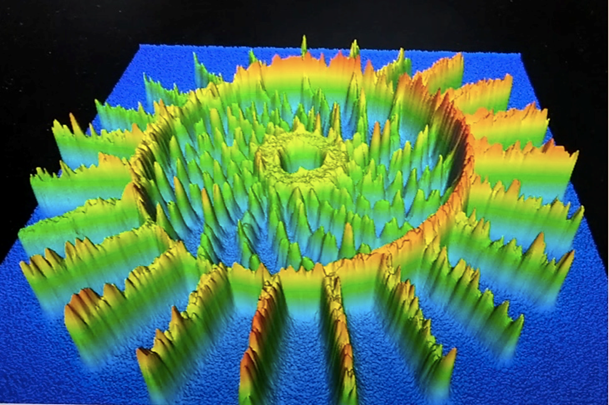
• Every Calibur3 incorporates an advanced and well-established, high-speed CMOS camera working in the NIR range and operating at four megapixels at 100 FPS, up to a maximum of 25,000 FPS at small resolution. The IR camera is calibrated to measure temperatures in the range of 600°C to 1500°C in order to provide absolute temperature measurements and cooling rates as well as identifying phase changes. In this way the IR camera can provide real time temperature mapping—temperatures calculated in real time via GPU processing. Moreover, measured temperatures can be presented in 3D for improved visualization, and the resulting plot can be interactively panned, zoomed, and rotated—also in real-time.
This type of thermal mapping can be used to monitor part dimensional accuracy, powder spreading during the build, energy absorption, and any out-of-plane defects that are not visible to the naked eye. This capability is particularly advantageous for rapidmaterial development.
• The structured light scanning system featured in the Calibur3 is based on the synchronization of a second CMOS camera and a light projector system. This system permits multiple fringe patterns to be projected onto the build area and captured by the camera. As a result, the system can calculate the z-axis (height) of every point on the build and thus produce an accurate height surface map of the powder bed. Any out-of-plane defects, on any layer in the build—caused by powder spreading or part swelling, for instance—can then be easily detected and quantified.
This system allows post-build defect and quality analysis to assist with process development, but Wayland’s technology roadmap will see this integrated into closed-loop machine control algorithms during the next couple of years.
• The backscattered electron detector—or electron imaging—process is able to detect the primary electrons (i.e., those emitted directly from the electron gun) that have been scattered back from the nuclei of atoms in the target material. Different element compositions and phases will interact differently with the electrons and thus appear distinct within the build chamber. The BED process can also detect localized ionization in the vicinity of the meltpool. This capability is unique to Wayland Additive’s NeuBeam process and the active-charge neutralization system.
This monitoring process provides useful data about the element composition and the grain structure within the parts, which can be analyzed and used to support traceability and demonstrate internal quality of the parts.
In short, Wayland Additive has prioritized the production requirements of quality and traceability for complex metal parts, which has been achieved with a dedicated and intelligent approach to IPM. Not only does this comprehensive monitoring approach greatly improve the quality of the parts off the machine, but it also specifically supports and improves operator experience. For the first time, operators can monitor the full process, including the cooling cycle, which can be altered to change the microstructure of parts to suit their needs.
NeuBeam is the most transparent metal additive manufacturing process to date, offering full traceability and eliminating the black-box approach to AM that has dominated the industry for so long.

Wayland Additive
Wayland Additive was born out of a high precision engineering team with a long and distinguished pedigree in the semiconductor industry, where electron beam widths are measured in nanometers and process instabilities are unacceptable. The use of and experience with eBeam technology in semiconductor manufacturing indicated that its use in additive manufacturing could be improved. Since 2015 a team of eBeam experts from the lithography world began to coalesce around solving the single most serious problem inherent in the eBeam AM process, the charging of the powder.